Semiconductor
![]() _Semiconductor_Pre-processing Phase_Pre-processing PhaseB
_Semiconductor_Pre-processing Phase_Pre-processing PhaseB
Pre-processing PhaseB
We will reward consumers with the best quality.
- Etching Process
- This is a process to remove unnecessary parts selectively to form a circuit pattern using chemicals or reactive gas. In order to make a circuit pattern on a wafer, unnecessary parts are removed selectively using chemicals (wet type) or corrosive gas (dry type). Leaving developer remaining parts, other parts are eroded. After finishing the etching, the photo sensitive solution is also removed with sulfuric acid solution. This process is similar to the process making a copperplate print. In the process making a copperplate print, a picture is drawn on a copperplate with a sharp gimlet after applying and smoking paraffin (photosensitive solution of semiconductor) on the copperplate. The gimlet peels off the paraffin. Then, a corrosive chemical solution is applied (etching process of semiconductor). When washing off the chemical and paraffin, a picture is completed. This process in semiconductor is almost same to the process of copperplate manufacturing.
- Ion Implantaion Process
- By accelerating impurities in a part connected to a circuit pattern to fine gas particles and infiltrating them into the inside of wafer, features of electronic material and device are created and this impurity injection is accomplished by diffusion process by diffusing and injecting the impurity particles into the inside of wafer in a hot electric furnace
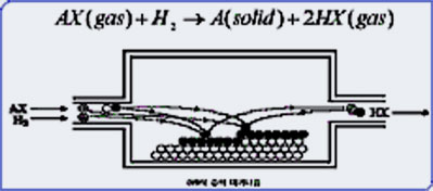
- CVD: Chemical Vapor Deposition
- This is a process to form a insulation membrane or conductive membrane by depositing particles formed by chemical reaction between reactive gases.
CVD: Chemical Vapor Deposition
This is an engineering technique to make a film such as silicone on a board during manufacturing process such as an integrated circuit. This is used to make silicone oxide membrane, silicone nitrogen film, and Amorphous Silicon. Because it uses chemical reaction in the manufacturing process, it is also called as CVD (Chemical Vapor Deposition). This is a technology to deposit a desired film on a board surface by injecting reactive gas into a vacuum reactor and adding appropriate active and heat energy to induce a chemical reaction. As a representing method to form insulation, metal, and organic film on semiconductor surface, it has characteristics such as relatively smaller pollution compared with the existing wet type electric gilding, more rapid deposition rate than other coating methods, and free controlling ability of the cover layer growth rate, so is applied widely in various industries currently. The deposition process is described by phases as follows. The first phase is that injection gas moves to a board surface to be deposited. The second phase is that the materials to be deposited are nucleated and grown via surface diffusion and reaction. Finally, volatile byproducts are removed to outside.
The thickness of film formed by this CVD process is diverse from several ㎚ to several tens ㎛ and it is very important to produce even deposition film over whole surface of wafer. Hydrogen is mainly used as a reducing gas and chlorine, fluorine, and brome gas are widely used as reactive gas. Deposition methods corresponding to CVD includes MOCVD (Metal-Organic Chemical Vapor Deposition), PECVD(plasma enhanced chemical vapor deposition), and LPCVD(Low Pressure Chemical Vapor Deposition) device. .
The thickness of film formed by this CVD process is diverse from several ㎚ to several tens ㎛ and it is very important to produce even deposition film over whole surface of wafer. Hydrogen is mainly used as a reducing gas and chlorine, fluorine, and brome gas are widely used as reactive gas. Deposition methods corresponding to CVD includes MOCVD (Metal-Organic Chemical Vapor Deposition), PECVD(plasma enhanced chemical vapor deposition), and LPCVD(Low Pressure Chemical Vapor Deposition) device. .
| LPCVD | MOCVD | PECVD | ALD | |
|---|---|---|---|---|
| Characteristics | Inorganic source |
Metalorganic source |
Low temp. | 단원자층 제어 |
| Process Temperature | ~600℃ | ~400℃ | <400℃ | |
| Process Pressure | 0.1~10 torr | 10~760 torr | 0.01~10 torr | 0.01~760 torr |
| Deposition reaction type | Surface reaction+ Vapor | Surface reaction+ Vapor | Surface reaction+ Vapor | Surface reaction |
| Step Coverage | Excellent | Good | Good | Excellent |
| Particle Contamination | Normal | Normal | Normal | Good |
| Thickness Controlling Factor | Gas supply,, temperature, time, etc. |
Gas supply, temperature, time, etc. |
Gas supply, temperature, time, etc. |
Process cycle number |
| Composition Controlling | Difficult | Difficult | Easy |
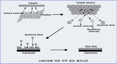
PVD(Physical Vapor Deposition)
A method to deposit a film by physical process different from CVD is referred to PVD (Physical Vapor Deposition). It is distinguished from CVD according to the method through which the material intended to be deposited are passed to be transformed to a board. Namely, when the desired materials are deposited on a board, the case that transformation process from gas to solid state passes through chemical change is classified as CVD and the case that passes through physical change is classified as PVD. As an apparent difference in the process is to make and blow off the desired material to be deposited into gas phase, high vacuum state is required. In other words, high vacuum state is required to prevent the problem that the material can not reach the board by colliding with other gas molecules or is transformed to solid losing energy during the process arriving on the board
ALD(Atomic Layer Deposition)
The deposition methods corresponding to PVD includes Sputtering, E-beam evaporation, Thermal evaporation, L-MBE (Laser Molecular Beam Epitaxy), and PLD (Pulsed Laser Deposition). Both PVD and CVD are used in semiconductor process or other industries. However, generally in case of PVD, it is used in high quality film or nano-structure, but the equipment is expensive and its deposition speed is low by requiring high vacuum. CVD is used in depositing a film or nano-structure in broad area at high speed. Sometimes, CVD may materialize a quality comparable to that of PVD, but in most cases, PVD can obtain high quality deposition surface when required device is equipped.